Microchip Technology
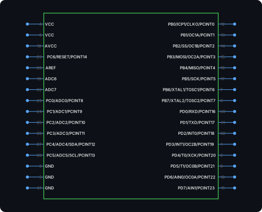
ATmega328P-AU
8-bit AVR microcontroller, the chip on the Arduino Uno, in a 32-lead TQFP.
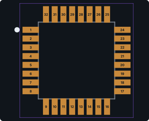
TQFP-32, 7 × 7 mm, 0.8 mm pitch · 32 pins · 32 pads
Pin map and all exports →Footprint generators usually make you type in the package dimensions yourself. PartSpark reads the mechanical drawing and recommended land pattern from the datasheet, applies IPC-7351B conventions, and shows you the resulting pad table (pitch, pad size, courtyard, pin 1) before you download. QFN, QFP, BGA, SOT, SOIC, connectors, and odd custom modules all go through the same path.
Live generator
Enter the part number or attach the package drawing. Check the pad dimensions on screen, then export the footprint and its matched symbol.
Parts database
Search the online catalog used by ProtoFlow. Look up a part number, LCSC code, or specifications. Searching does not use generation credits.
Source: PCB Parts · JLCPCB / LCSC. Keyword search covers indexed parts with at least 10 units in stock. Stock and prices may change; confirm on the supplier page. Selecting a result fills the generator and does not start a generation.
How to use it
[01]
Generate
Type the manufacturer part number, or attach the datasheet PDF (or a photo of the pinout and package pages) for unusual parts. A generation takes about a minute.
[02]
Check the land pattern
Compare pitch, pad size, row spacing, exposed pad, and pin 1 with the package drawing, using the pad table and the generator’s notes.
[03]
Export
Download KiCad .kicad_mod, EAGLE .lbr, an Altium .PcbDoc bundle, or the Allegro pad table and KiCad footprint for conversion.
Doing it by hand, or want to know what to check? Step-by-step guides: how to create a kicad symbol from a datasheet; how to turn a package drawing into a kicad footprint; how to check a generated symbol and footprint before fabrication.
Limits to know
The guide to checking a generated symbol and footprint before fabrication shows real cases where these limits mattered.
Example output
These were generated from the part number alone, then every pin and pad was checked against the manufacturer datasheet. Download the files and open them in KiCad yourself.
Microchip Technology
8-bit AVR microcontroller, the chip on the Arduino Uno, in a 32-lead TQFP.
TQFP-32, 7 × 7 mm, 0.8 mm pitch · 32 pins · 32 pads
Pin map and all exports →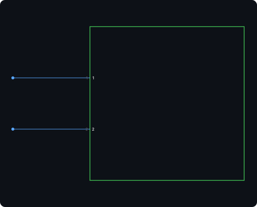

JST
2-pin vertical through-hole header from JST’s 2.0 mm PH series, the common battery and sensor connector.
Through-hole, 1 × 2, 2.0 mm pitch, vertical · 2 pins · 2 pads
Pin map and all exports →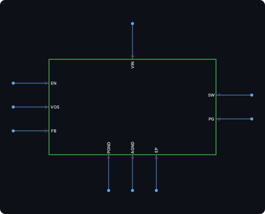
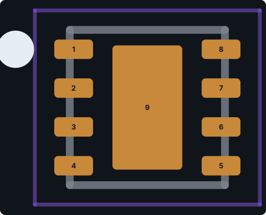
Texas Instruments
Texas Instruments 3 V to 17 V, 1 A synchronous step-down converter in a 2 × 2 mm WSON-8.
WSON-8, 2 × 2 mm, 0.5 mm pitch, exposed pad · 9 pins · 9 pads
Pin map and all exports →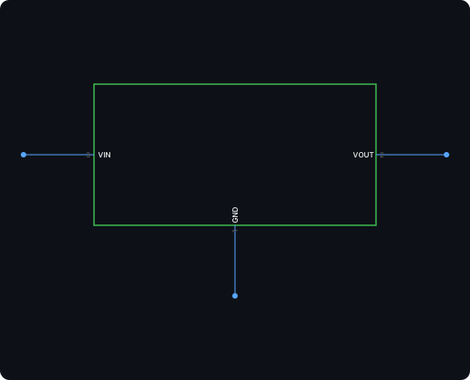
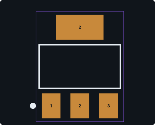
Advanced Monolithic Systems
1 A fixed 3.3 V low-dropout regulator in SOT-223.
SOT-223-3 with tab · 3 pins · 4 pads
Pin map and all exports →FAQ
Need a different tool? AI KiCad Part Generator · Altium Designer Part Generator · EAGLE Library Generator · Cadence Allegro PCB Footprint Generator · Datasheet to Schematic Symbol Converter · AI Schematic Symbol Generator · KiCad Symbol Generator · KiCad Footprint Generator