1. Use the land pattern, not the package outline
A package drawing has two kinds of numbers. The mechanical outline describes the part: body size, lead width, lead length. The recommended land pattern (TI calls it “Example Board Layout”) describes the copper you put on the board. Build the footprint from the land pattern. Copper is deliberately larger than the leads so the solder can form a fillet.
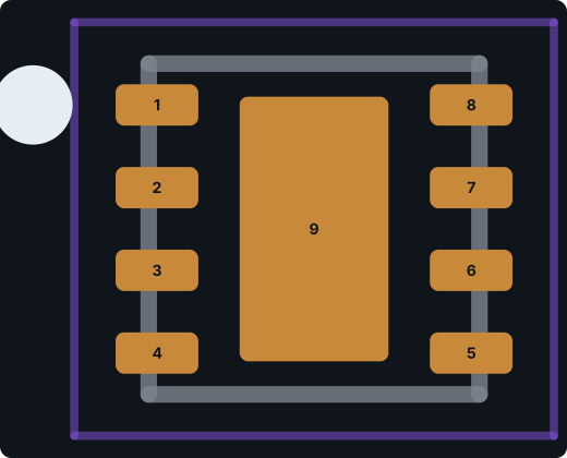
Numbers in parentheses on TI land patterns are reference values for your CAD. The DSG0008A example gives everything needed:
| Callout | Value | Meaning |
|---|---|---|
| 8X (0.5) | 0.5 mm | Pad length (across the row) |
| 8X (0.25) | 0.25 mm | Pad width |
| 6X (0.5) | 0.5 mm | Pitch between adjacent pads |
| (1.9) | 1.9 mm | Distance between the two pad-row centers |
| (0.9) × (1.6) | 0.9 × 1.6 mm | Exposed thermal pad |
| Ø(0.2) VIA TYP | 0.2 mm | Optional thermal vias (note 5: optional) |
2. Compute pad centers from the footprint origin
Put the origin at the package center. With rows 1.9 mm apart, pad centers sit at x = ±0.95 mm. Four pads per side at 0.5 mm pitch sit at y = −0.75, −0.25, +0.25, and +0.75 mm. Pin 1 is top-left in the top view, and numbering runs counter-clockwise: 1 to 4 down the left side, 5 to 8 up the right. The thermal pad is pad 9 at the origin.
That is exactly what PartSpark generated for the TPS62160DSG: eight 0.5 × 0.25 mm pads at x = ±0.95 mm and a 0.9 × 1.6 mm pad 9. Opening the .kicad_mod and reading the pad positions is the fastest way to confirm a footprint against a drawing.
3. Handle the exposed pad: number, net, vias, paste
- Number: give it a pad number the symbol also has (here 9), so it lands on a net instead of floating.
- Vias: TI marks the 0.2 mm thermal vias optional. Leave them out of the library footprint and add them in layout where the board needs the heat path, or include them if every board will.
- Paste: a full paste opening on a large thermal pad can float the package. TI’s stencil example prints about 87% coverage on pad 9. The generated footprint has a full-size paste opening, so reduce or split it if you follow TI’s stencil.
4. When the datasheet has no land pattern
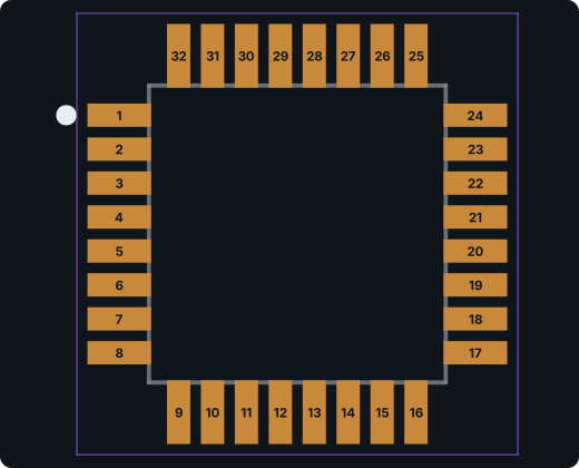
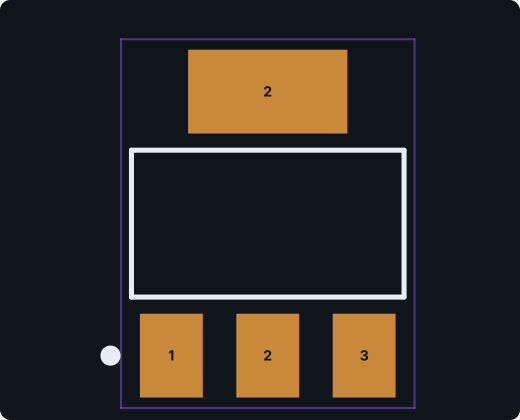
Many datasheets give only the package outline. Microchip’s ATmega328P datasheet dimensions the TQFP-32 body and leads but doesn’t recommend copper, and the AMS1117 datasheet gives a SOT-223 outline and nothing more. Then you fall back to IPC-7351B calculations or a proven footprint for the same JEDEC package.
PartSpark does the same and says so. For the ATmega328P it built standard TQFP pads (1.50 × 0.55 mm, rows 8.40 mm apart). KiCad’s own TQFP-32 uses 1.475 × 0.55 mm at 8.325 mm, so the two are close but not identical. For the AMS1117 it reused the copper of KiCad’s official SOT-223-3_TabPin2. Read the generator’s notes: they tell you which case you are in.
5. Courtyard, silkscreen, and fab layers
- Courtyard (F.CrtYd): the keep-out around the part, typically 0.25 mm beyond the body or pads, whichever is larger.
- Silkscreen (F.SilkS): an outline that stays off the pads, plus a pin-1 mark you can see after assembly.
- Fab layer (F.Fab): the true body outline for assembly drawings.
6. Save and register in KiCad
Save the .kicad_mod into a folder whose name ends in .pretty, then add that folder under Preferences → Manage Footprint Libraries. If you also use a generated symbol, give the library the nickname its Footprint field expects (ProtoFlow.pretty for PartSpark parts) or edit the field.