1. Find the pin table, not just the pinout drawing
Datasheets usually show the pinout twice: a package drawing with pin numbers, and a Pin Functions table with names, directions, and descriptions. Work from the table. It is where the manufacturer says which pins are inputs, which are open drain, and what the exposed pad connects to.
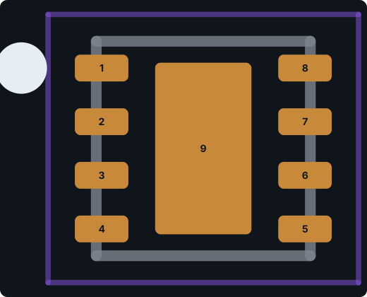
For the TPS62160 (TI SLVSAM2E, section 6) the table lists eight pins for the DSG package, plus an exposed thermal pad that “must be connected to AGND.” That last note matters for both the symbol and the footprint.
2. Turn each row into a pin with an electrical type
KiCad’s ERC checks connections using each pin’s electrical type. Map the datasheet’s I/O column to KiCad types: supply and ground pins become power input, I becomes input, O becomes output, and open-drain outputs become open collector. Getting PG right is the difference between ERC flagging a missing pull-up or saying nothing.
| Pin | Name | Datasheet I/O | KiCad electrical type |
|---|---|---|---|
| 1 | PGND | — (power ground) | Power input |
| 2 | VIN | I (supply) | Power input |
| 3 | EN | I | Input |
| 4 | AGND | — (analog ground) | Power input |
| 5 | FB | I | Input |
| 6 | VOS | I | Input |
| 7 | SW | O | Output |
| 8 | PG | O, open drain | Open collector |
| 9 (pad) | EP | Connect to AGND | Power input |
3. Place pins so the schematic reads well
Convention keeps schematics readable: power at the top, ground at the bottom, inputs on the left, outputs on the right, with related pins grouped. Pin numbers must match the footprint pad numbers exactly, including the exposed pad. If the symbol calls it 9 and the footprint calls it EP, the pad is left unconnected in layout.
Give the exposed pad its own pin rather than hiding it. A visible pin 9 on the AGND net makes the connection explicit on the schematic and in the netlist.
4. Fill in the fields
- Reference: U for ICs, J for connectors.
- Value: the full orderable part number (TPS62160DSG, not TPS62160).
- Footprint: library nickname plus footprint name, for example ProtoFlow.pretty:WSON-8_DSG0008A_2x2mm_P0.5mm_EP_NoOptionalVias.
- Datasheet: a working link to the manufacturer PDF. Check it still opens; we found one generated link that had gone offline.
5. Import the .kicad_sym into KiCad
- Preferences → Manage Symbol Libraries → add the .kicad_sym as a global or project library.
- Preferences → Manage Footprint Libraries → add the folder holding the .kicad_mod (it must end in .pretty) with the nickname the Footprint field uses.
- Place the symbol, run ERC, then Update PCB from Schematic. If the footprint doesn’t appear, the nickname in the Footprint field doesn’t match your library table.
Doing it with PartSpark
Typing “TPS62160DSG” into the generator produced the pin map above in a little over a minute, including the open-drain PG and the exposed pad tied to AGND, plus a matching footprint. Your job becomes step 2 in reverse: read the pin map against the datasheet table and correct anything in plain English. The generated files are on the TPS62160DSG example page.